Implementation of Analog Signal Waveform Based on FPGA
1 Introduction
Waveform generators have been widely used in various fields such as communication, control, and measurement. Waveforms such as sawtooth, sine, and square waves are often used in circuit design and debugging. With the rapid development of electronic technology, digitalization is gradually becoming the development trend of the electronics industry, and each company has expanded its products in the direction of digitization, integration, and miniaturization. As we all know, digital electronic products have their irreplaceable advantages, such as small size, high level of integration, and strong anti-interference ability. However, the digital circuit can only process the pulse waveform well, that is, only the square wave formed by l and 0 is well processed. The signal of continuous gradation cannot be processed well, and this is precisely the advantage of the analog circuit. . In this paper, the digital circuit is combined with the analog circuit, that is, the control signal of various analog waveforms is generated by the FPGA, and then the gradual signal is processed by the analog circuit, so that the chord can obtain various clear waveforms.
2 oscilloscope display principle
First, briefly explain the display principle of the oscilloscope to better understand the working process of the hardware circuit. During the entire display, the oscilloscope needs to always be in the "XY" position, ie the waveform of the waver is a superimposed composite display of the X-axis and Y-axis input signals. It can be seen that in general, the variable input on the x-axis is the signal frequency, and the variable input on the Y-axis is the signal amplitude. Therefore, when a signal frequency value of 5KHz is input on the x-axis and a DC voltage amplitude of 0V is input on the Y-axis, a bright spot is displayed at the position where the oscilloscope is located at (5KHz, 0V); similarly, if in Y A 5V DC voltage amplitude is input to the axis, and a 0Hz signal frequency value is input on the x-axis. A bright spot is also displayed at the oscilloscope at (0Hz, 5V); if on the x-axis and Y-axis When the input is 5KHz or 5V, the bright spot will appear on the oscilloscope (5KHz, 5V). In this way, if the two axes are assigned without interruption, a clear and continuous signal waveform can be displayed on the oscilloscope.
3 hardware design
This paper mainly introduces the analog waveform design of step wave and sawtooth wave in common signals. Their analog circuit is simple to implement and the actual output waveform is clear. The hardware circuit in the scheme is mainly composed of a south DSP, an FPGA and a peripheral chip. The DSP is used to control the output position and amplitude of the analog waveform; the peripheral chip is used to generate an analog waveform, such as using two DAC0832 to generate two voltage signals, One is used to control the height of the sawtooth wave and the other is used to control the height of the step wave. The FPGA performs the logic programming of the various control signals required.
Here, the FPGA uses ALTERA's 10K10 series of programmable logic devices. ALTERA's FLEX 10K series devices are the industry's first embedded programmable logic devices. They are flexible logic element array architectures that utilize a common gate-sea architecture to implement general logic functions, and also use dedicated silicon to achieve scale. Large dedicated features. Compared to standard gate arrays, the embedded silicon is implemented on silicon, requiring less silicon area and higher system speed. The FLEX 10K family not only provides high density, high speed and system integration, but also includes multiple 32-bit buses, 6144 bits of RAM space inside a single device, and supports both serial and parallel configuration and online simulation of JTAG mode. These features make the FLEX IOK family of devices one of the most widely used programmable logic devices. Correspondingly, the development tool used is MaxplusII programmable logic development software. MaxplusII is used as the software tool of EDA to realize powerful logic functions. It also has the advantages of short cycle, high integration and reasonable price. Moreover, since the logic modules of the circuit are implemented in the FPGA, they have good portability and easy maintenance, and are convenient for future system improvement. At the same time, this further reduces the board area and greatly increases the integration of the circuit. In this design scheme, the FPGA is mainly used to perform control programming of various analog waveforms, and various logics are generated as their control signals. Among them, the block diagram of the logic control in the FPGA is shown in Figure 1. It can be divided into three parts, and the coarse sweep and fine sweep signals are the control signals of the sawtooth wave.

Figure 1 Functional block diagram of the control signal module in the FPGA
The working process of the FPGA is as follows: First, the input 32KHz clock signal is divided by a counter to generate a narrow pulse signal of 1600 Hz, which serves as a scan trigger signal of the external analog waveform generating circuit on the one hand, and as a sawtooth control signal on the other hand. The work start signal, that is, every time the signal arrives, other function modules are activated to generate the required control signals according to the required timing. It can be seen from Fig. 1 that when the frequency of 1600 Hz comes, the input clock (2MHz) of the fine sweep counter and the coarse sweep counter will be turned on, and the initial loading process of both will be started, and then the input pulse will be subtracted by this initial value, when the subtraction overflows. The output will generate the desired scan signal. At the same time, the signal is also used to turn off the respective input clock signals until the next 1600 Hz arrives. When the 8-bit initial value of the subtraction counter is changed by a logic operation, the timing of the output signal is changed correspondingly to the 1600 Hz signal. This logic allows you to control the appearance of various analog waveforms, allowing you to control the display position of various waveforms on the oscilloscope. The initial value of the subtraction counter is changed by an 8-bit latch, that is, the address line of the DSP, the read/write signal line, and the access control line of the I/O space are logically operated as an 8-bit latch. The strobe signal is then used to write 8-bit data to the subtraction counter using the program.
The staircase wave control signal is completely implemented by a software program, that is, according to its various timings, different data is written into the FPGA for latching at different times, and then output through the D flip-flop to control the generation of the signal. In order to meet the needs of the system, a logic for controlling the width variation of the waveform is also designed to generate a pulse sequence of different widths required for display. The T. is performed by two square wave signals of different frequencies and one D flip-flop. The output terminals D and D respectively perform logical AND operations, and then perform a logical OR operation, and then change the output state of the D flip-flop through a program, thereby obtaining an output pulse having two widths.
4 Experimental results
4.1 step wave waveform
Here, a brief introduction to the specific generation process of the staircase waveform. First, we need to design an analog circuit that can generate four different DC voltages, so that it can output DC voltages of different amplitudes under different combinations of control signals. The analog circuit has a total of four control signal inputs that control the combined inputs through a software program of the DSP. When the combined state is "0001", the circuit will output a DC voltage of 4V, and when the combined state is "0010", the circuit will output a DC voltage of 5v. At the same time, it is also necessary to give the output position of its response. In this way, when the program loop changes the combined state of the input, in the double trace display mode, the staircase waveform as shown in Figure 2 can be obtained, and this waveform is input to the x-axis of the oscilloscope, and the corresponding oscilloscope There are four highlights in the position.
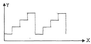
Figure 2 staircase waveform
In the actual project, two kinds of non-pulse width conversion are performed in the FPGA through the DSP program, and the signal of the required pulse width is set to an appropriate width through the external monostable flip-flop, and then passed through the differentiation and integration circuit. The waveform shown in Figure 3 is formed. This waveform is input to the oscilloscope's Y-axis and set to the "XY" file. Finally, four bright lines are displayed. When the narrower pulse in (a) is input to the Y-axis, the dwell time of the different amplitude points is basically kept consistent by the program, so that the corresponding bright line of the display is relatively uniform; When the wider pulse in b) is input to the Y-axis, it is programmed to stay at the highest amplitude point for a longer time than at other amplitude points, which makes the corresponding bright line top than the bright line. The other parts are brighter, and finally a bright line graph shaped like a match head is displayed on the oscilloscope.

Figure 3 two widths in the pulse signal
4.2 sawtooth waveform
Similarly, a sawtooth waveform can be generated in accordance with the interphase concept. As can be seen from the above, the FPGA will output a pulse of 1600 Hz as the trigger signal of the external analog circuit. Under its action, the analog circuit will generate a scan signal with a length of 100 us, which will be used as the input signal of the X-axis on the oscilloscope, and will be 0V. The DC voltage is input to the Y axis. Then, according to the display principle of the oscilloscope, since the input of the Y-axis is 0V, the bright spot can only appear on the x-axis, and the input signal of the x-axis is a continuous signal with a fixed frequency value, so that it will be displayed on the oscilloscope. A waveform that continually draws a baseline on the x-axis. Then, through the DSP software program to control the analog circuit, generate a continuously varying DC voltage value, and then output to the oscilloscope's Y-axis, you can get the sawtooth waveform on the oscilloscope, as shown in Figure 4.
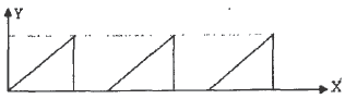
Figure 4 sawtooth waveform
5 Conclusion
Here, the FPGA is used to form a core control circuit for generating a control signal of an analog waveform, and a peripheral circuit is used to generate a sawtooth wave and a staircase wave. Through experimental observation, the generated waveform is clear and free from clutter interference. It shows that the analog circuit can process the gradual signal well, which fully reflects the advantages of the analog circuit. Moreover, in practical engineering, the sawtooth wave and the staircase wave are reasonably used to generate various analog waveforms required for the project. As long as some of the circuits are slightly modified, they can be applied to other applications.
Silicone Container,Silicone Wax Jar,Wax Container Ball,Silicone Wax Container
Dongguan Chakou Silicone Products Co, Ltd , https://www.waxmaidwholesale.com